Protected IP with the possibility of extending protection
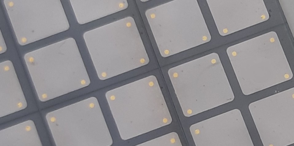
Photo: archive of inventors/Institute of electrical engineering SAS
Competitive advantage
- possibility to use lower quality semiconductor materials (CdTe, GaAs, CdZnTe, SiC, InP, etc.);
- more precise measurement result (unaffected by defective areas);
- simpler construction;
- higher production yield;
- the result is obtained directly, without the need to correct the measured values;
- significant financial savings during operation;
- reduction of demands on the amount of control electronics for reading the detector;
- possibility to connect to only one reading unit (instead of a large number);
- each produced large area detector is functional (in case of defects in the material, the total detection area will only be reduced by max. 10 – 30% ).
Use of technology
- in nuclear energetics (spectrometry, dosimetry);
- wherever there are sources of ionizing radiation of natural or artificial nature;
- in space applications.